

Silicon
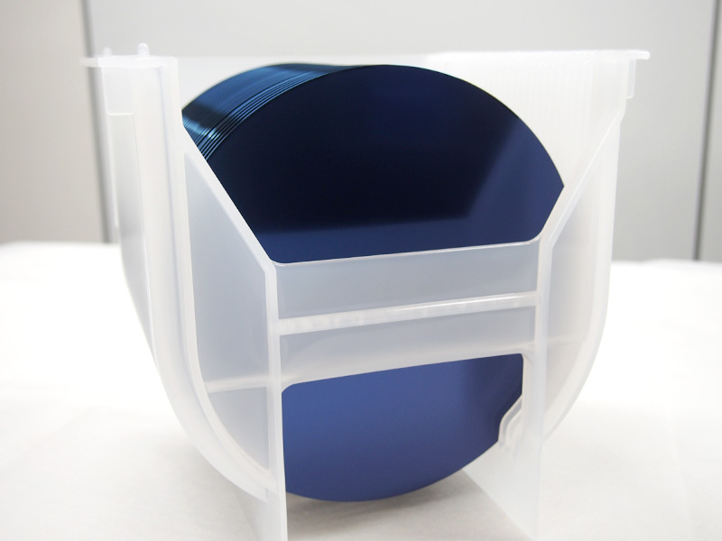
Silicon Wafers
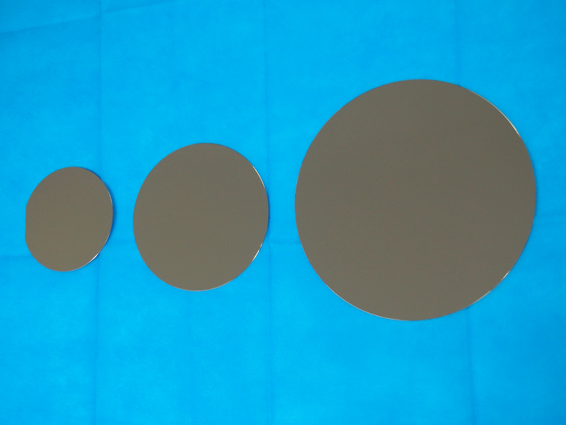
We supply silicon wafers as substrate for fabricating semiconductor devices according to the specifications meeting
customers’ needs.
If you look for silicon wafers with special specifications, please feel free to consult with us.
Standard Specifications
Please refer to the specifications below for inquiries.
| Diameter | 2″ | 3″ | 4″ | 5″ | 6″ | 8″ | 12″ |
|---|---|---|---|---|---|---|---|
| Growth Method |
CZ or FZ | CZ or FZ | CZ or FZ | CZ or FZ | CZ or FZ | CZ or FZ | MCZ |
| Crystal Axis |
<100> or <111> | <100> or <111> | <100> or <111> | <100> or <111> | <100> or <111> | <100> or <111> | <100> |
| Conductivity Type |
P or N | P or N | P or N | P or N | P or N | P or N | P or N |
| Resistivity | Arbitrary values between 0.01 and 1,000 Ω-cm |
Arbitrary values between 0.01 and 1,000 Ω-cm |
Arbitrary values between 0.01 and 1,000 Ω-cm |
Arbitrary values between 0.01 and 1,000 Ω-cm |
Arbitrary values between 0.01 and 1,000 Ω-cm |
Arbitrary values between 0.01 and 1,000 Ω-cm |
Arbitrary values between 0.01 and 1,000 Ω-cm |
| Thickness | 280±25 μm | 380±25 μm | 525±25 μm | 625±25 μm | 625±25 μm | 725±25 μm | 775±25 μm |
| Surface Finish |
Polished | Polished | Polished | Polished | Polished | Polished | Polished |
| Backside Finish |
Etched | Etched | Etched | Etched | Etched | Etched | Polished |
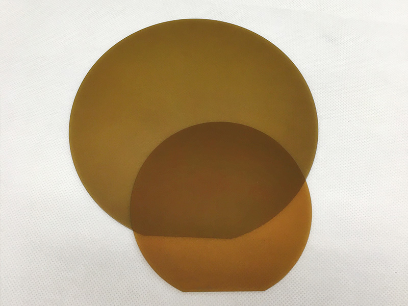
Silicon Wafers with a Thin Film
- Silicon Wafers with an oxide film formed by thermal oxidation
- 4”φ~12”φ silicon wafers with an oxide film formed by wet or dry thermal oxidation, whose thickness ranges between 500Å and 3μm are available.
- Silicon Wafers with a metal film formed by sputtering
- 4”φ~12”φ silicon wafers with a film of any of the following metals are available.
Kinds of Metals: Ta, Tan, Ti, TiN, W, WSi, TiW, Cr – Film thickness range; 300Å ~ 3,000Å
Cu, Al, Al-Cu(1%), Al-Si(1%), Al-Si(1%)-Cu(1%)– Film thickness range; 500Å ~ 1.5μm” - Silicon Wafers with a metal film formed by vacuum evaporation
- 4”φ~12”φ silicon wafers with a film of any of the following metals are available.
Kinds of Metals: Pt, Ru, Pd, Au, Ag, Co, Ni, NiSi, Al-Alloy – Film thickness range; 1,000Å ~ 2.0μm
Specially Processed Silicon Wafers
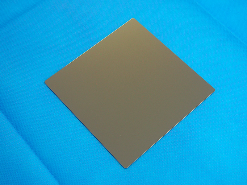
Silicon wafers processed with a variety of special processing techniques are available in arbitrary sizes for parts
used for semiconductor material/device manufacturing equipment.
・Special Processing: Processing into a square, Spot facing, Drilling, Processing into a cylindrical shape,
Down-sizing, Thinning and so on
Silicon Scraps

Silicon scraps are available for recycling and for use as additives.
・Top or tail of silicon ingot
・Off-grade silicon ingot
A Variety of Compound Semiconductor Materials
Various types of compound semiconductor materials for the substrate of power devices, LED, and semiconductor lasers
are available.
・SiC (Silicon Carbide)
・GaN (Gallium Nitride)
・GaAs (Gallium Arsenide)
・InP (Indium Phosphide)
Other Material
・Sapphire for the substrate of LED and optical window is available.